On PCBs

After digging deep into the manufacturing capacity side of printed circuit boards (PCBs), I wanted to assess a high level view of the PCB value chain. Given that PCBs are integral to most, if not all, electronic devices today, I want to share my learnings.
Overview
What are PCBs and why are they important?
A printed circuit board (PCB) is an electronic assembly that uses copper conductors to form electrical connections between components. PCBs provide mechanical support for electronic components so that a device can be mounted in an enclosure. Essentially, a PCB provides 1) interconnectivity between electronic components that allows an electronic device, such as a light switch, to work, 2) rigid support to hold components, and 3) compact packaging that can be integrated to an end electronic device.
To appreciate a PCB, we should understand the prior iteration of electronics design. In the past, electronics were designed from small integrated circuits and distinct components connected with wires. Electronic components were packaged by attaching individual wires to components and by mounting those components to a rigid substrate (i.e. bakelite, which was used to replace the top ply on plywood sheets). The industry formed conductive paths by soldering metal components to wires, which, as you may anticipate, amplifies the number of wires within a design when a circuit is large. This made debugging quite difficult and manufacturing sluggish.

In the above image, we have a simple single-sided PCB to illustrate the various layers of the stack-up:
- Substrate: The substrate is a dielectric material that will determine the mechanical, thermal and chemical properties of a circuit board. PCBs commonly use a glass fiber reinforced epoxy resin with a copper foil bonded to one or both sides.
- Copper layer: This is a thin foil of copper that is laminated to the board with adhesive and heat.
- Solder mask: The solder mask insulates the copper traces from contacting any solder or metal.
- Silkscreen: The silkscreen layer contains numbers, letters, or symbols to give guidance to people handling the board.
With the basic understanding of the PCB stack-up, we can then progress to understanding the various types of PCBs. There are three main types of PCB construction:
- Single-sided: Single-sided boards have the electronic components on one side of the substrate.
- Double-sided: A double-sided board may be used when the number of electronic components balloons too much for a single-sided board. Electrical connections between the circuits on each side of the board are made by drilling holes through the substrate and plating the inside of the holes with a conducting material.
- Multi-layered: A multi-layered board has a substrate composed of layers of printed circuits separated by layers of insulation. The components on the surface connect to a certain circuit layer through plated holes.
There are various other types of PCBs including rigid PCBs, rigid-flex PCBs, flex PCBs, metal-core PCBs, and ceramic PCBs, among others.
Designing PCBs
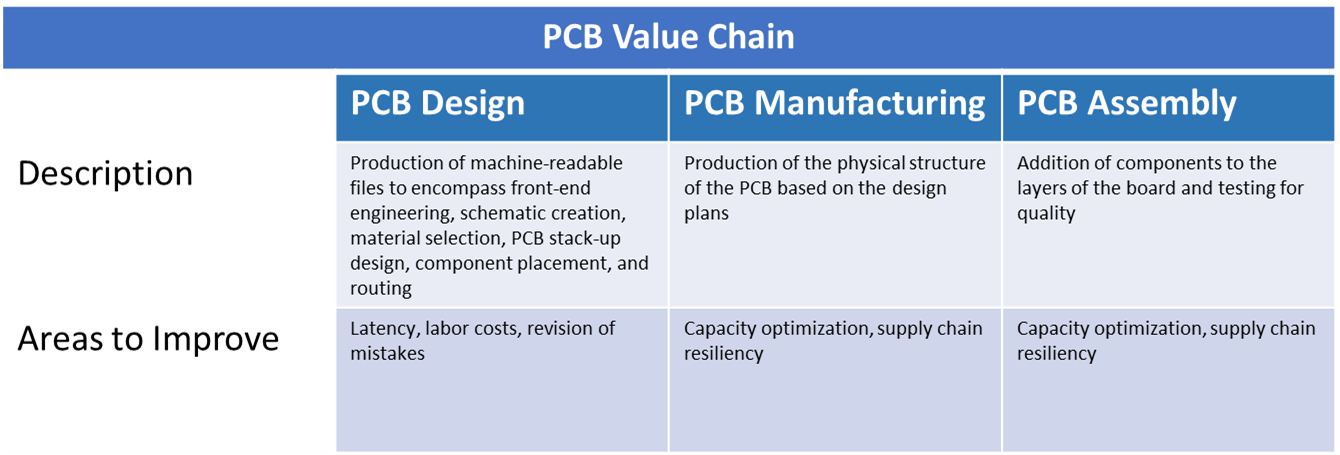
Designing a PCB positions itself as a prominent step within the electronics value chain. The most basic circuit board is even designed with specialized software packages. When diving into this piece of the value chain, we will see the usage of a PCB layout, which is a CAD drawing displaying the location of all elements that will show up on both sides of a PCB. The PCB design process goes as follows:
- Front-end engineering: Major components of the board are selected and basic circuit diagrams are created to design the functionality
- Schematic creation: Electrical computer aided design (ECAD) software translates basic circuit diagrams into electronic drawings that denote electrical connections between components
- Material selection / PCB stack-up design: Laminate materials selected and stack-up designed to account for various layers, routing channels, and material properties
- Component placement: Components placed and arranged in a new PCB layout
- Routing: Route traces between components
- Design review: Evaluation via manual inspection or use of post-layout simulation tools of design to ensure absence of unresolved problems
- Physical design to machine-readable files: WIth a completed design, one can create the standard manufacturing files for automated fabrication
The current set of design tools for PCBs has room for improvement in terms of latency and labor. Latency refers to the layout of the PCB file, which can range from days to months. Manual labor is baked into the process as schematics and mechanical constraints have to be agreed upon by the stakeholders of the PCB.
Manufacturing PCBs
PCB manufacturing produces the physical structure of the PCB based on the design plans. Below is an oversimplified list of the process to do so:
- Make the substrate
- Drill and plate the holes
- Create and print circuit pattern on the substrate
- Laminate board materials
- Add protective coating to surface or solder masking
- Printing logos or other markings on surface
Room for improvement within this piece of the value chain is to optimize electronics manufacturing services capacity for contract manufacturers (CMs) as a nontrivial portion of factories are underutilized, leading to dents within the underlying cash flow of CMs. In addition, reliable procurement of components became more top of mind since the pandemic stressed the supply chains.
Assembling PCBs
PCB assembly (PCBA) is when the manufacturer adds components to the layers of the board. Depending on the contract manufacturer (CM), there is a wide range of automation within the assembly line. In the optimal case, boards can move from machines that place electronic components in the proper location in the circuit. Some components, however, may be too large or oddly shaped for automated placement and must be manually placed and soldered. Testing is then conducted.
Similar to PCB manufacturing, optimizing capacity here will be important for the CMs who need to maximize the bottom line. For the OEMs who request the PCBA, they are looking for reliable sources of manufacturing capacity.
Market Landscape
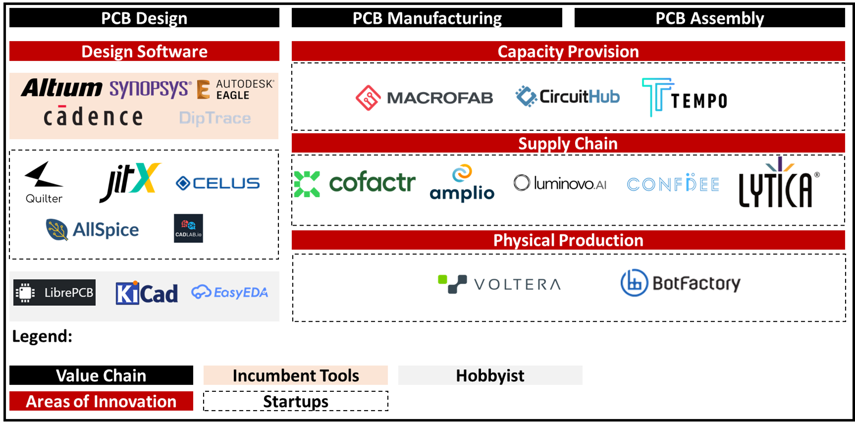
Above is a market landscape (by no means comprehensive) of the players addressing the various steps within the PCB value chain. The landscape was conducted with an angle towards the young startups innovating within this space.
For design software, I see various players innovating along the themes of version control, generative outputs via code, and automation of schematic/layout outputs.
For PCB manufacturing and assembly, the topics of innovation include solutions in capacity provision, supply chain (procurement, compliance, visibility, etc.), and physical production. Capacity provision encompasses companies who are providing flexible capacity in the form of software, marketplace dynamics, or even a streamlined in-house play to meet OEM demand. Players within the supply chain side offer visibility, intelligence, logistics or compliance surrounding procurement of components. Innovators of the physical production of PCBs and their components essentially speeds the process of creating the board.